高密度柔性Mini-LED背光模组——2020神灯奖申报技术
摘要: 高密度柔性Mini-LED背光模组,为深圳远芯光路科技有限公司2020神灯奖申报技术。

项目名称: 高密度柔性Mini-LED背光模组
High-Resolution Flexible Mini-LED Back-Lighting Module
申报单位: 深圳远芯光路科技有限公司
综合介绍或申报理由:
本项目利用全球首创的“新型封装材料+特制设备+捆绑工艺”的全套技术方案,可实现柔性基板上Mini-LED超高密度的巨量封装(目前点间距可达到P0.3mm,极限可到P0.2mm左右,单片模组尺寸最大可至10英寸),且整个最终的背光模组更加轻薄(300微米以下)和可弯曲。该产品为业界唯一超高密度&超轻薄的柔性Mini-LED背光模组产品。
另外,本项目的技术壁垒高,在新型封装材料、设备及工艺方面都具有自主知识产权,并完全形成闭环系统:可实现超低温倒装封装技术,节省能耗;并采用新型的卷对卷及面阵式巨量封装设备,提高生产效率;其可靠性与良品率能与成熟的LED封装工艺媲美,并且达到传统焊膏无法实现的超小点间距;可在线返修机AOI,并捆绑巨量转移设备;可极大提高生产速度、降低成本,可真正实现低成本、及高分辨率的Mini-LED 柔性背光标准尺寸模组的规模化量产,有望在全行业中得到推广,推动Mini-LED行业的快速发展。
In this project, the whole technical scheme is including new packaging materials, special designed facilities and the new bonding process, which is initiated by the world. It can be used to realize the ultra-high resolution Mini-LED back-lighting module on the flexible substrate. Its point spacing can reach P0.3mm at current mass-production capability, the limitation can go down to P0.2mm in future. And its the maximum size of single module can reach 10 inches. Moreover,the final backlight module is much lighter with higher flexibility than before because of the ultra-thin flexible substrate (<30 microns). This new product with such kind of excellent acteristic is the one and only in the market.
In addition, the technical barriers of this project are high. It has independent intellectual property rights in new packaging materials, equipment and technology, which forms a closed-loop system completely.It advantages are shown as below:
(1) It can realize ultra-low temperature flip-chip packaging to save energy consumption and be able to use such kind of low cost flexible material as the substrate;
(2)It can adopt the roll-to-roll production scheme to improve production efficiency; (3)
(3) Its packaging reliability and yield can be comparable with mature LED packaging technology, and the cost remain as before;
(4) It can reach the ultra-small point spacing which the traditional solder paste cant achieve, to realize the ultra-high resolution;
(5)Its final special designed facility can integrate the online repair system, the AOI system, and the mass-transfer system in one production line, which can make mass packaging come true.
To conclude, this technology can greatly improve the production speed, reduce the cost, and truly realize the high-resolution Mini-LED flexible back-light module with different standard size and pitch size. It will be expected to be promoted in the whole industry to speed up the development of Mini-LED industry.
主要技术参数:
代表性Mini-LED显示模组主要参数如下:
点间距: < P0.9mm ,极限到P0.3mm,与现行LCD像素点一一对应
模组尺寸:2-10英寸
模组厚度:< 300um
亮度:视乎分辨率来定,与传统封装无差别
生产效率:200K/H
良品率:99.99%
可靠性 :连续4000小时点亮无损
The main parameters of the representative Mini LED display module are as follows:
Point spacing: < p0.9mm, limit to p0.3mm, corresponding to current LCD pixel points one by one
Module size: 2-10 inches
Module thickness: < 300um
Brightness: no difference from traditional packaging
Production efficiency: 200K / h
Yield Rate: 99.99%
Reliability: lighting for 4000 hours continuously without damage
与国内外同类产品或同类技术的比较情况:
本项目产品是市场上唯一超高分辨率且柔性的Mini-LED背光模组。该终端产品形态开辟了一个全新的蓝海市场,不会与现有大型LED厂直接进行竞争,竞争优势明显。产品形态非常新,性能优异,成本低,竞争力强,市场空间广阔;另外,我们的技术壁垒是完全形成了闭环系统,包括核心新型封装材料,搭配特制的设备及捆绑工艺的模式,可以持续保持产品及市场能够领先。
(1)市场上所有的封装技术不能实现超高分辨率(超高密度)的封装,目前技术极限只有P0.75mm,本项目的技术可以实现极致的P0.2-0.3mm左右;
(2)市场上所有的封装技术都不能实现超薄超柔的基板封装,目前市场上没有真正的柔性LED显示模组或背光模组的存在;
(3)市场上所有的封装技术都不能实现低成本、高密度、无缝拼接的Mini-LED背光模组。因为常见的PCB基板厚且笨重,点间距缩小的时候PCB非常贵,无法实现低成本、高密度的模组;且玻璃基板的LED背光模组也存在着加工尺寸难的问题;而柔性基板却可以随意拼接,且厚度非常薄,可降低最终LCD的厚度。
(4)市场上所有的封装技术都不能实现卷对卷、超高效率的真正巨量封装,本项目在未来1-2年内可以实现600-1000K超高的UPH,效率提高,成本可以大幅下降。
因此,本项目产品形态非常新,性能优异,成本低,竞争力强,市场空间广阔;另外,技术壁垒完全形成了闭环系统,包括核心新型封装材料,搭配特制的设备及捆绑工艺的模式,可以持续保持产品及市场能够领先。因此,该技术值得关注,提高中国Mini-LED可制造水平,并有机会实现超高清Mini-LED显示屏。
This product is the only ultra-high resolution and flexible Mini-LED backlight module in the market. The terminal product form has opened up a new blue ocean market, will not directly compete with the existing large LED factories, with obvious competitive advantages.
(1) All packaging technologies on the market cannot achieve ultra-high resolution (ultra-high density) packaging. At present, the technical limit is only P0.75mm, and the technology of this project can achieve the ultimate P0.2-0.3mm;
(2) At present, there is no real flexible LED display module or backlight module in the market;
(3) All the packaging technologies in the market can not realize the low-cost, high-density, seamless splicing of the Mini-LEDmini LED backlight module. Because the common PCB substrate is thick and bulky, PCB is very expensive when the point spacing is reduced, so it can not achieve low-cost and high-density modules; and the LED backlight module of glass substrate also has the problem of processing size, and the flexible substrate can be spliced at will, and the thickness is very thin, which can reduce the thickness of the final LCD.
(4) All the packaging technologies in the market can not achieve volume to volume, ultra-high efficiency and really huge package. In the next 1-2 years, the project can achieve 600-1000k ultra-high UPH, with improved efficiency and significantly reduced cost.
Therefore, the product form of this project is very new, the performance is excellent, the cost is low, the competitiveness is strong, and the market space is broad; in addition, the technical barrier has complet
经济评价分析:
Mini-LED具有高分辨率、高亮度、省电及反应速度快等特点,被视为新一代显示技术,吸引苹果、三星、LG、索尼等大型企业布局发展。2019年称为Mini-LED显示元年,该领域有望成为继LED照明产业发展之后能够迅速崛起的版块之一,有望带动整个LED行业的改变,包括LED芯片、封装及应用全产业链的全面升级,使整个LED产业或将进入新一轮发展周期。
目前Mini-LED的应用主要有两大方向:直接显示屏市场及背光应用市场。据高工LED预测,2018-2022年,Mini-LED市场规模将从不足10亿元增长至300亿元,当前利亚德、洲明科技、雷曼光电纷纷推出点间距在P0.6-P0.8mm的样品,由于良品率低及成本高等原因并未量产,其可制造问题限制了行业的发展。
相比而言,封装难度低的Mini-LED背光应用则有望率先成为Mini-LED的主战场。Apple已经宣布将在2020年三季度的Pad新产品中使用Mini-LED背光模组,国产手机厂商进一步跟进,随后会在大屏LCD中应用,例如高清电视机等。但当前Mini-LED背光市场的量产还未成熟,一是无法实现更高分辨率的背光,二是良品率低成本太高。
而本项目的实施可以为Mini-LED背光应用提供更轻薄、分辨率更高的柔性背光模组,打开全新的市场;在未来1-2年内,还可以实现大面积可拼接的、点间距在P0.4mm左右的、超高清RGB Mini-LED柔性显示屏。同时该项目的实施,可为低成本高可靠的超高分辨率的Mini-LED巨量封装提供全新的行业解决方案,解决现阶段封装厂无法解决的可制造问题,最终可极大推动Mini-LED行业的发展。
技术及工艺创新要点:
1. 高精度柔性基板封装;
2. 超高密度封装技术;
3. 快速巨量封装技术;
4. 卷对卷封装技术;
5. 材料+设备+工艺捆绑,技术首创
6. 该技术具有极大的拓展性:可拓展到超高分辨RGB Mini-LED直显产品;可拓展到任意高密度面阵式芯片的产品,例如红外传感器等;可拓展到任意基板类型的产品,例如Al,Si,玻璃,PCB等
1. High precision flexible substrate packaging.
2. Ultra high density packaging technology
3. Fast and huge package technology
4. Roll to roll packaging technology
5. New material, special designed facility, and carefully matched bonding process window, the whole technology loop is the one and only in industry
6. The technology has great expansibility: it can be expanded to ultra-high resolution RGB Mini led direct display products; It can be expanded to any high density planar array chip products, such as infrared sensors; It can be expanded to any substrate type products, such as Al, Si, glass, PCB, etc.
获奖、专利情况:
LED芯片及其制备方法 申请号:2019111259807
其他专利正在申请中,设计材料,设备及工艺方法
LED chip and its preparation method
Application No.: 2019111259807
Other patents are pending, design materials, equipment and process methods
申报单位介绍:
深圳远芯光路科技有限公司于2019 年9 月成立,公司是市场唯一超高密度&超轻薄的柔性Mini-LED背光模组供应商。公司的背光模组以柔性PI材料为基板,搭载0408型号及以下的倒装Mini-LED芯片,可实现点间距在P0.5mm以下及不同标准尺寸的倒装封装模组,为业界首创。公司由朱玲博士发起,与刘二壮博士天使投资联合创,注册资金为100万(工商变更中)。
Shenzhen YuanXin optical Technology Company was established in September 2019. It is the only supplier of ultra-high density and ultra light, thin and flexible Mini LED backlight module in the market. The backlight module of the company is based on flexible PI material, equipped with 0408 and below flip chip Mini led, which can match flip package modules with point spacing below p0.5mm and different standard sizes, and it is the first in this industry area. The company was jointly founded by Dr. Zhu Ling and Dr. Liu Erzhuang with a registered capital of 1 million yuan.
朱玲博士是LED芯片设计、加工制造、封装应用及可靠性领域专家,有近12年LED行业研究与开发的工作经验。她曾经在世界顶级LED公司CREE研发部效力5年,曾带领开发团队发布近30款大功率LED封装产品,引领了全球的技术方向,多次获国内外奖项;其中CXA-HD系列全面突破业界当时产品性能(分级光效最高达到189lm/W),获2015年中国“最佳照明芯片/封装金奖”和2014年美国“最佳灯具设计奖”。另外,在香港大学攻读博士期间,她师从香港大学H. W. Choi教授(Micro-LED 领域的先驱者,Micro-LED的发明人之一Martin Dawson教授的学生),在LED及Micro-LED芯片设计、制造与应用领域积攒了丰富的经验,发表了相关学术期刊论文近40余篇,申请专利近20项,授权5项。她曾开发了基于微纳结构的大功率LED芯片,短波长的微盘GaN固体激光器,激光微纳加工系统及基于此系统开发的特殊形状 LED及薄膜LED芯片,超高显色指数(100)的可变色LED,高光效的垂直LED芯片等多种新型光电器件,同时也研究了低成本新型高效绿色无污染无铅量子点和碳量子点发光材料。此外,她近期还有多项发明,有望在行业中应用:例如基于全新的基于Mini-LED显示屏的巨量转移方法,可使固晶流程UPH能至少提高到600k,而目前市面上最好固晶机的UPH仅为180k。
刘二壮博士为LED、半导体行业专家,运营专家,现任美国Lam Research(全球知名半导体设备公司)集团副总裁,中国区总经理。刘博士拥有西安交大本科,英国丹迪大学博士,美国哈佛大学博士后,新加坡国立大学MBA等学历,曾任CREE公司中国总经理、美国泛林半导体设备研发有限公司中国区副总经理、上海先进半导体有限公司运营总监,曾获2013年“中国LED行业十大领军人物”称号。刘博士的行业地位能为公司来带行业关注。
除此之外,公司其他核心团队成员专业领域涵盖了LED 芯片、封装、产品及量产等多个领域,团队成员在LED行业及管理方面均有10+年以上经验,有非常强的产业化背景及工程能力。
最后,公司的成立得到了许多行业前辈的支持与帮助,其技术顾问团队包括以下成员:
-香港的H. W. Choi 博士(Micro-LED 领域先驱者)
-严群博士(千人专家,显示屏领域专家,前长虹首席科学家)
-马昕博士(千人专家,新能源电池领域专家)
-闫春辉博士(千人专家,LED芯片领域专家)
-吴懿平教授、博导(国内电子封装、制造领域专家)。
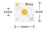
产品图片:


凡注明为其它来源的信息,均转载自其它媒体,转载目的在于传递更多信息,并不代表本网赞同其观点及对其真实性负责。